
I'm having some trouble stitching such a large and blurry (due to the lack of landmarks and the small focus depth of my microscope) images, so I will post the images in parts.
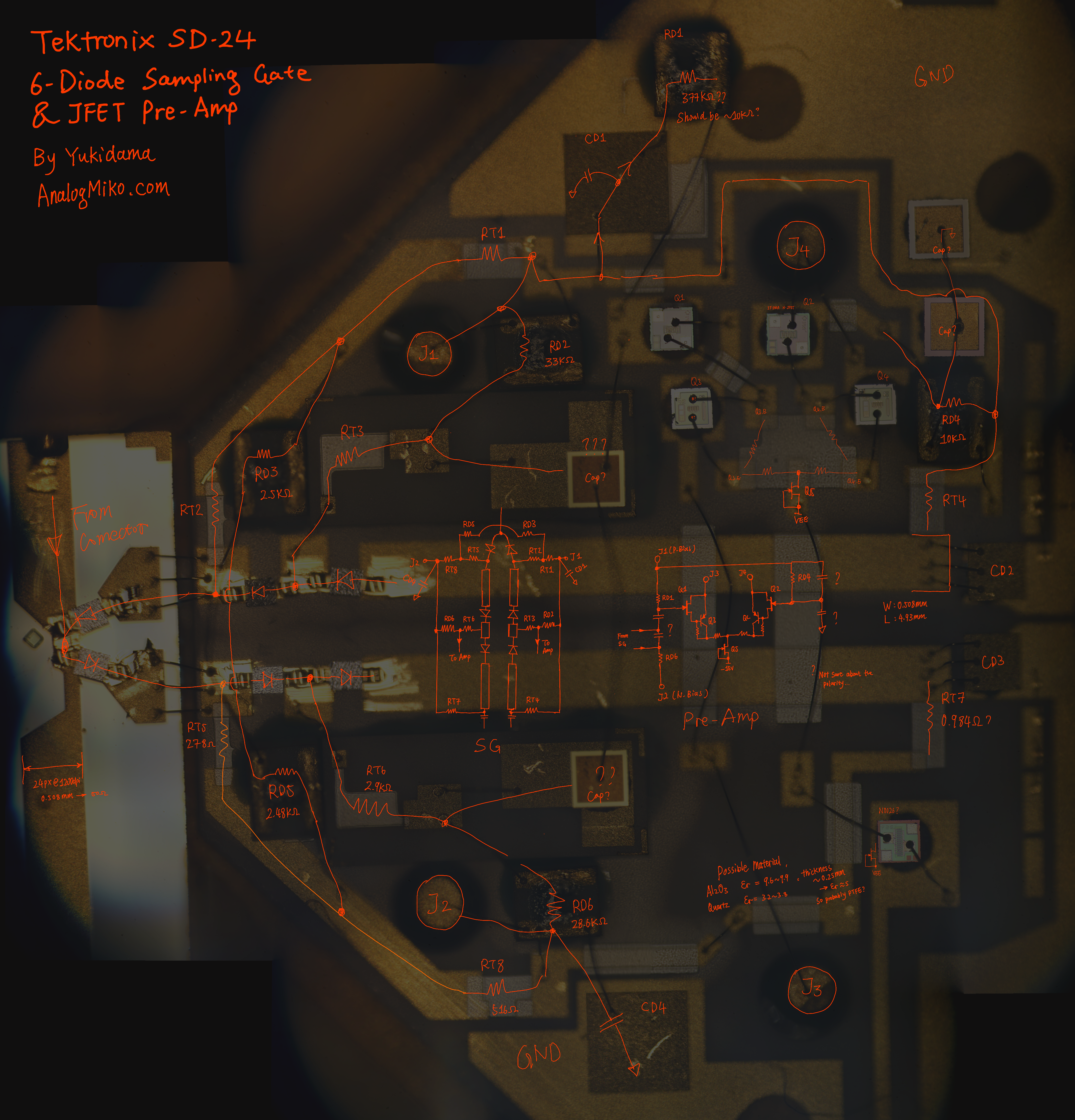
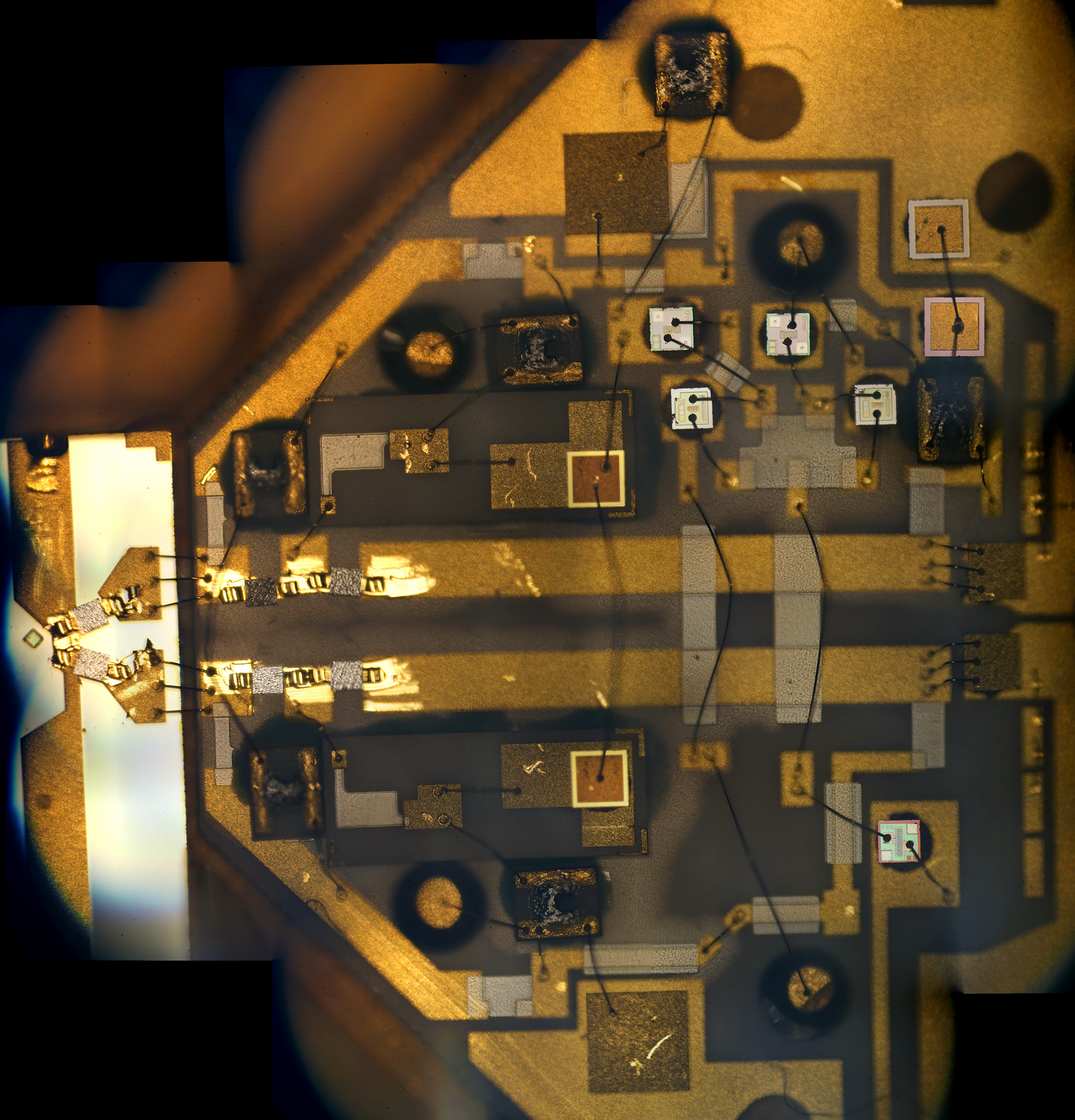
Sampling Gate Circuit of Tektronix SD24
It's very similar to that of the original SD-4 and SD-6 heads. In close proximity to the sampling bridge there's a JFET-based preamp to bring the signal out from this board. Unlike SD-4 and SD-6, this design doesn't appear to have blow-by compensation.
With the help of Google Image search, I was able to identify the JFET as IF140A. The BJTs are unknown.
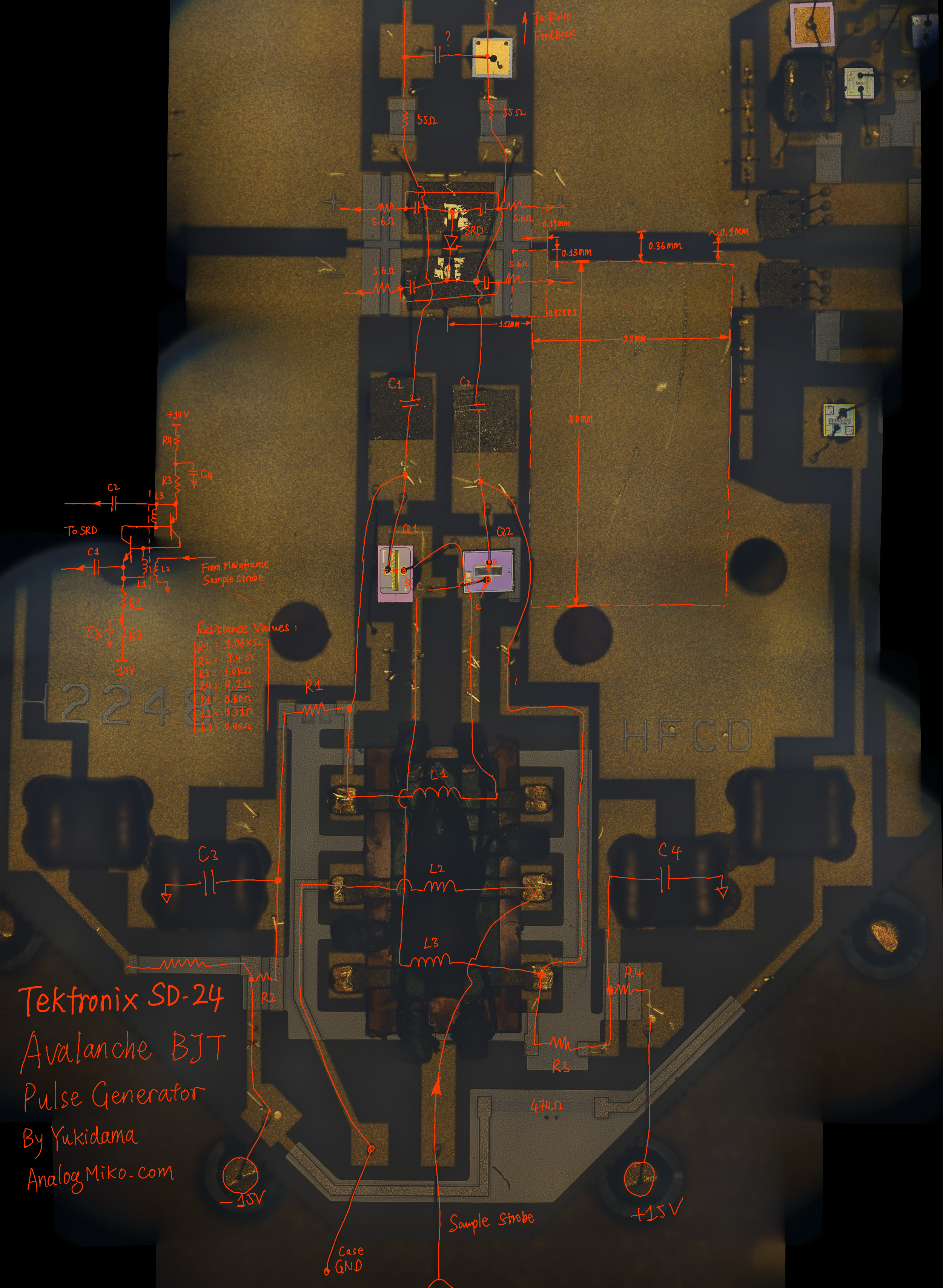
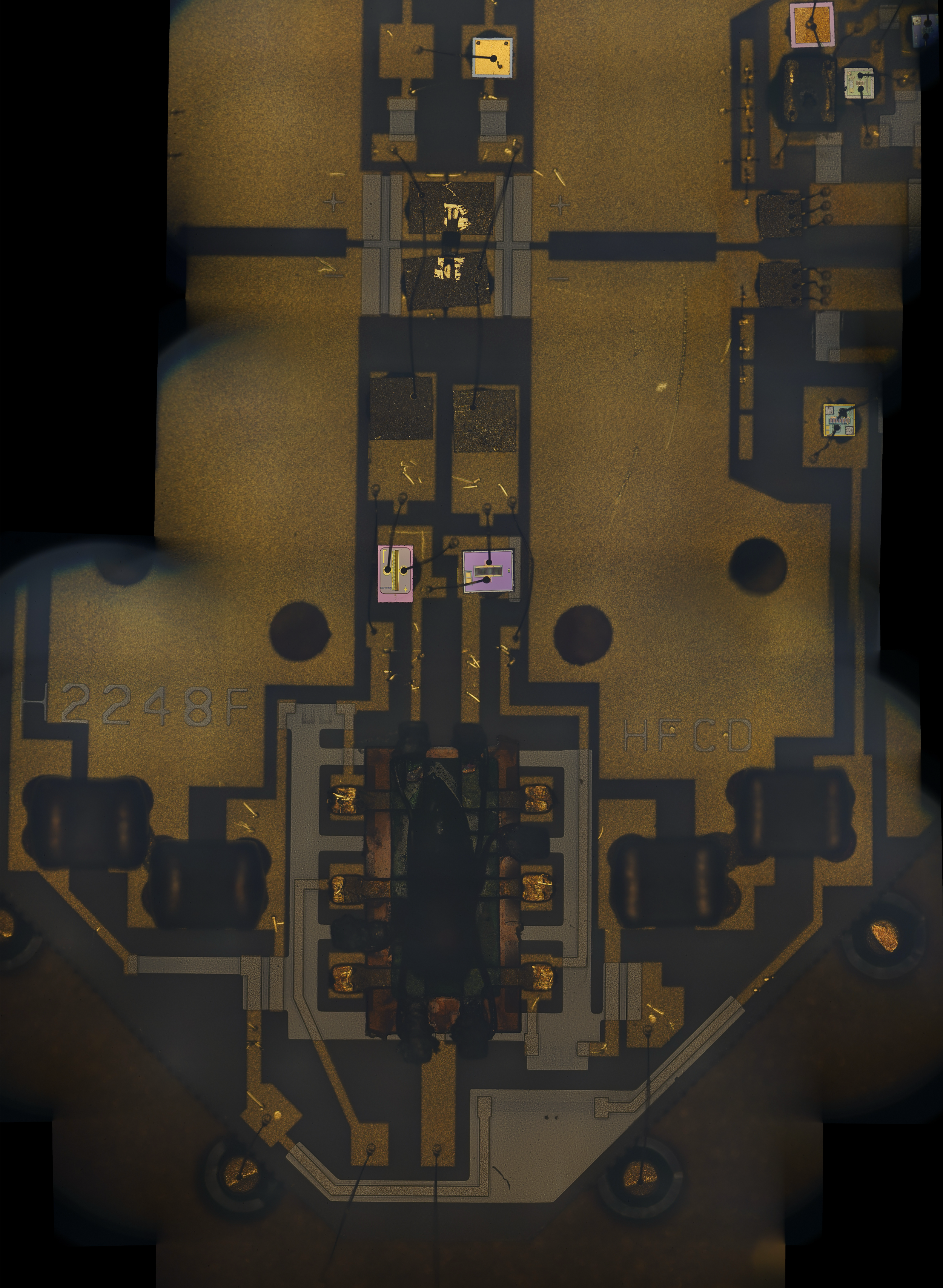
Avalanche + SRD Pulse Generator of Tektronix SD24
This is the pulse generator descibed in the previous post. Curiously this design uses a bipolar design with one NPN and one PNP. I'm not sure how the engineers managed to match them well enough to get a clean pulse out of this circuit. The SRD sits on two pieces of ceramic capacitors.
I couldn't identify the BJTs and the SRD. It seems that the NPN is a high speed type with emitter ballasting, very similar to everyone's favorite: BFG540.
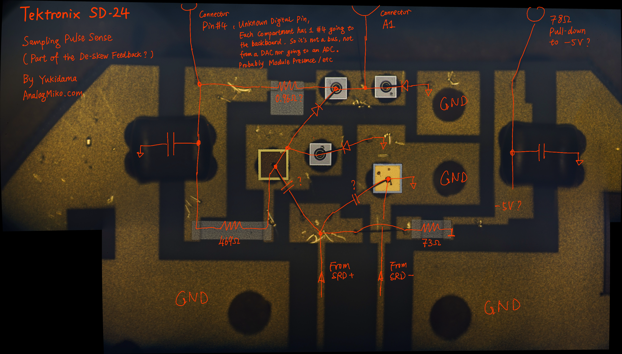
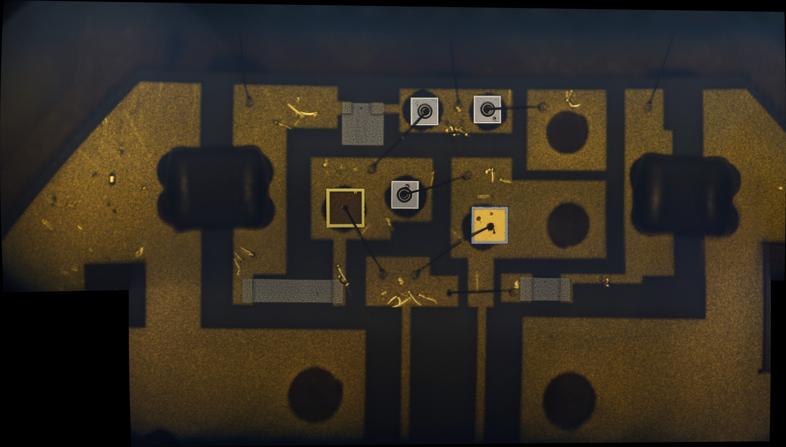
Pulse Feedback Circuit of Tektronix SD24
There's some additional passives near the ports of this RF module. They're going into one of the coaxial connectors of the module, and seems to be related to the "Strobe Sense" functionality mentioned in the service manual. I'm not sure exactly what this circuit does.
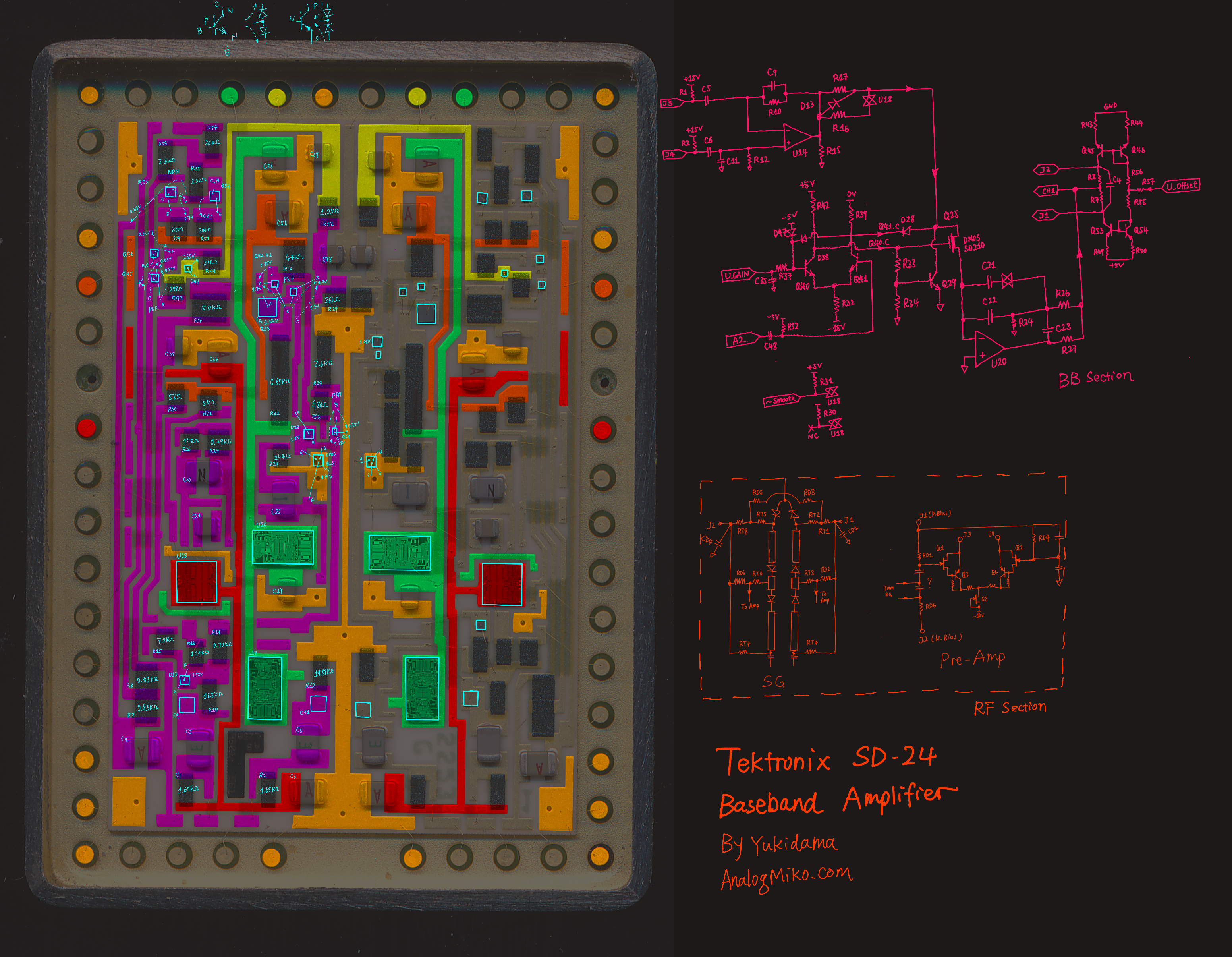
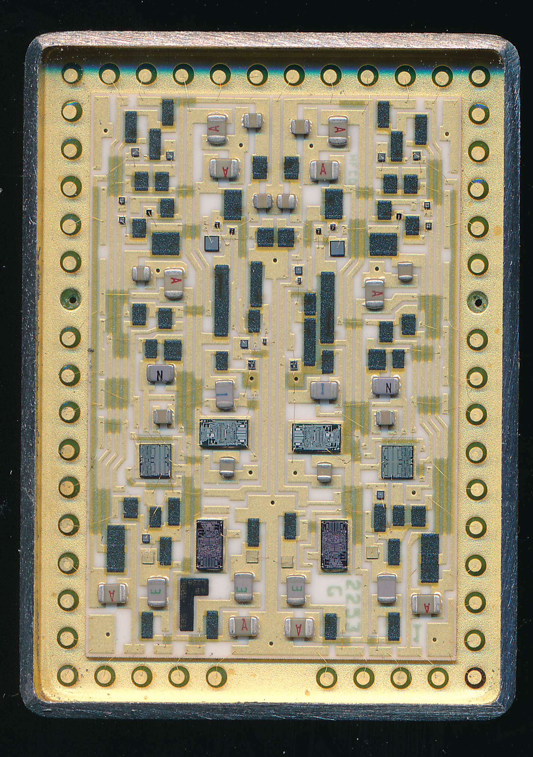
Baseband Amplifier Hybrid (165-2253-01)
AFAIK this hybrid is a common component for most of the SD series sampling heads. It provides the baseband amplification and offset adjustment for the sampled LF signal coming from the RF section.
I opened the metal can by grinding the edges on a piece of #120 sand paper. The image is scanned with a Canon 9000F Mark II, it's not as clear as Leo Bodnar's scans[Leo], but It's sufficient. Note that the design is quite different from what Leo has scanned, so there might be different revisions of this hybrid.
I'm not too sure about the polarities of those BJT transistors and the diodes, so this figure is just for information and there's no guarantee that it will work. It's because I didn't want to destroy this module by poking around in there. This module is still functional after I put everything back together.
The LF signal came into the hybrid from J3 and J4 of the RF block. There's an input pre-amp (U14) built around a Harris HA5160 OpAmp. Followed by a variable gain amplifier built with another HA5160 (U20) with a SD210 discrete DMOS as a variable resistance. The signal path has a variable loop gain implemented with what appears to be an analog MUX chip (U18) to implement the "smoothing" function[7S11].
Aside from the main signal path, there's a pair of current mirrors implemented with discrete transistors to provide bias for the diode sampling bridge through J1 and J2, and also buffer the offset-trimming DAC signal.
I'll talk more about the RF section and maybe the TDR pulse generator in the next post.
I took some dieshots during reverse engineering and have uploaded them to SiliconPr0n.