
The Tektronix SD series is a family of sampling heads for the 11800 series mainframes. These sampling heads are capable of capturing extremely high-frequency signals, with bandwidths ranging from 2.5 GHz (SD-14) to 50 GHz (SD-50). I'm amazed by the fact that engineers were able to achieve such high performance using the semiconductor technology available in the 1980s and always want to learn more about it, and eventually build one myself for fun. Starting from this article, I will present a detailed reverse engineering of the SD-24 sampling head, which has a bandwidth of 20 GHz and a built-in pulse generator capable of producing extremely fast edges for Time Domain Reflectometry (TDR) applications.
 Tektronix SD-24 with the Lid of the RF Section Removed
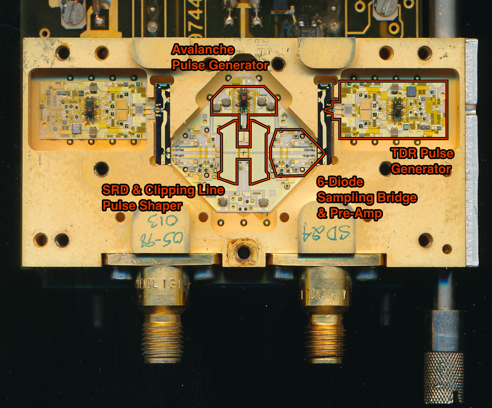 Overview of the Key Building Blocks of the RF Section
A sampling oscilloscope captures a repetitive high-frequency signals at effective sample rates as low as 100 kHz. You can find more information about them online - to put it short, it locks onto the repetitive signal and take repetitive samples at different time offsets, gradually building up a high-resolution representation of the waveform over many cycles. This greatly relaxes the requirements on quantization (i.e. the speed of the ADC) and data-rates, and it also makes impedance matching easier. Application-wise, sampling oscilloscope is what made the most cutting edge SerDes buses (USB, PCI-E, etc) and high-speed optical-electrical datalinks testable in very early stages of R&D, way before the technology is even mature enough to implement a transceiver IC.
However, generating a stable and ultra-fast sampling aperture is just as challenging as designing a real-time oscilloscope front end. As the first article in this series, I will provide a brief overview of the two most important building blocks of such a frontend: the diode sampling gate and the pulse generator.
The fundamental building block of a sampling oscilloscope is a fast sample-and-hold switch that can turn on and off within picoseconds. It “steals” a small amount of charge from the input signal and stores it on a capacitor, allowing the ADC to take much longer to digitize the signal. The time interval between the gate being fully off, fully on, and fully off again is called the aperture time. To achieve 50 GHz bandwidth, the aperture time must be less than 20 ps. Every digital oscilloscope since its inception has relied on such a sampling gate.
As a general rule in electronics, faster switching is achieved by minimizing physical size. (Note that in this context, fast means high bandwidth and low noise—a transmitter centered at 20 GHz with a data rate of 100 kbps is still considered slow.) Semiconductor engineers therefore strive to make the switching element as small as possible. In modern designs, MOSFETs with extremely short gate lengths are often used. Thanks to Dennard scaling, today’s MOSFETs can switch in picoseconds. However, this kind of sampling gate suffers from voltage limitations (typically less than 1 V), making it more fragile and distortion-prone. Moreover, such small MOSFETs were not available in the 1980s, before the advent of advanced lithography.
Instead of using MOSFETs, engineers of that era exploited the junction of a Schottky diode as the switching element. By controlling diffusion duration and doping levels, researchers in the early 1970s could already fabricate junctions only nanometers thick, achieving very high switching speeds even with relatively primitive fabrication technology. When the diode is forward-biased, it conducts and charges the hold capacitor; when reverse-biased, it stops conducting and isolates the stored charge. [HP Diode]
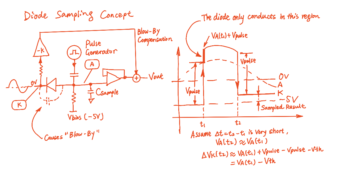 Illustration of the diode sampling process
The earliest implementations used a single diode as the sampling gate. This simple design had several limitations, leading to the development of two-diode sampling bridges and eventually the widely adopted four-diode bridge. The following example is a LTSpice simulation model of a basic 2-diode sampling bridge. You can download the simulation files and try it yourself here.
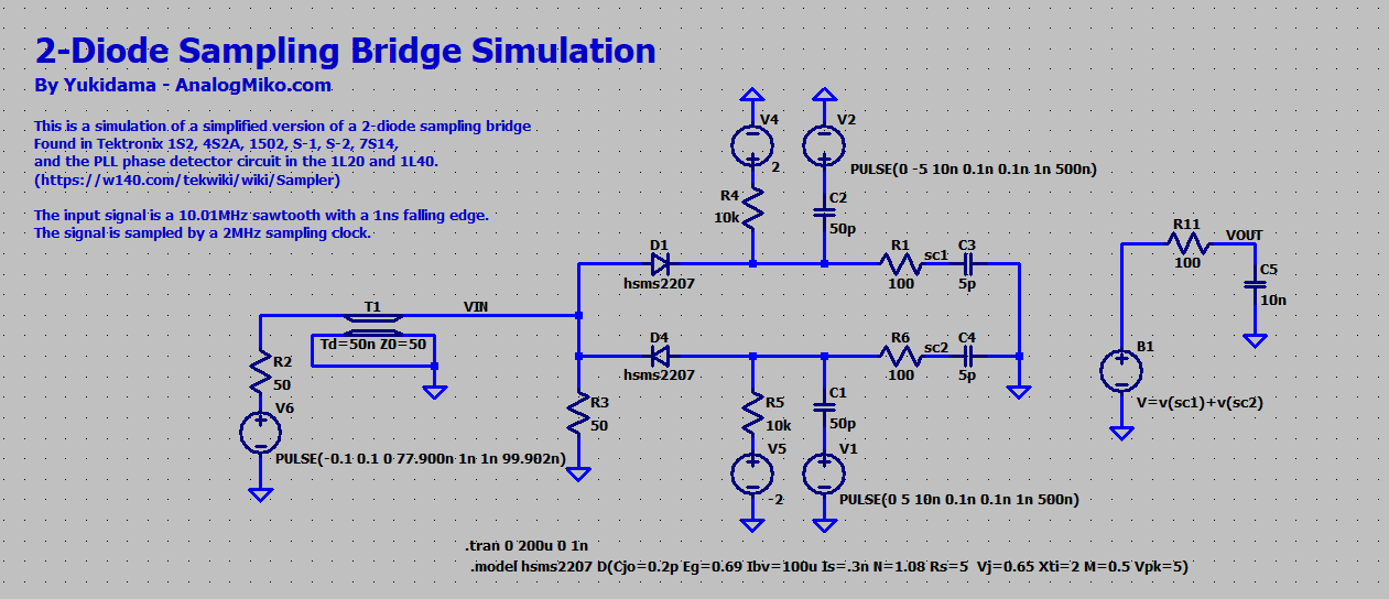 2-Diode Sampling Bridge Simulation File
Tektronix achieved approximately 5 GHz bandwidth with a two-diode sampling bridge in their S-2 sampling head, introduced in 1967. However, further increasing the bandwidth proved difficult, as it required an impossibly fast sampling pulse. A breakthrough came in 1968 with the introduction of the six-diode sampling bridge in the S-4 sampling head, invented by George Frye. He described the operation of this innovative circuit in detail in one of his publications and patents. [George Frye]
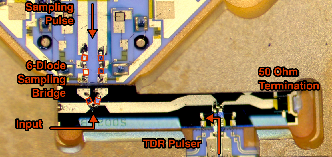 Photo of the 6-Diode Sampler from my Tektronix SD-24
In essence, a traditional sampling gate is like slicing a piece of cake (the input signal) with one chef and one knife—the chef must make two separate cuts to isolate a small piece. In the new design, the cake moves along a conveyor belt (representing the transmission line), and two chefs perform the cuts individually: one on the rising edge, the other on the falling edge. The conveyor belt effectively stretches time, allowing the second chef to make a much narrower and more precise cut.
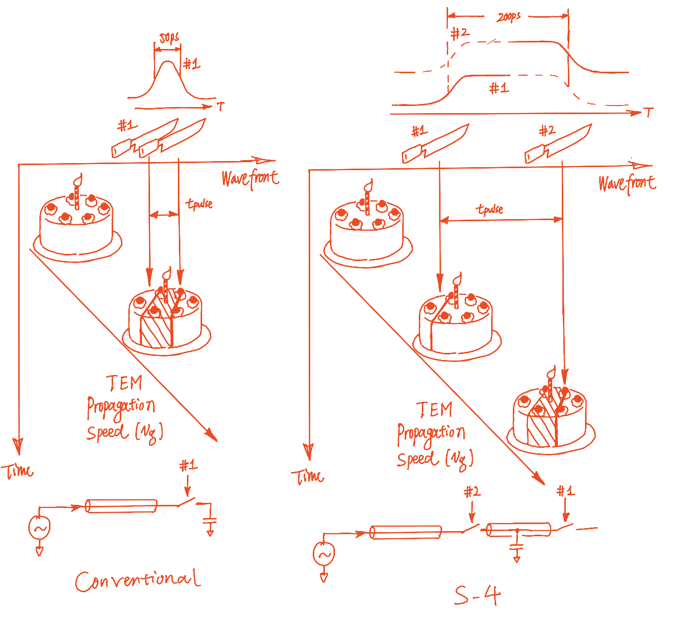 Analogy of the 6-diode Sampler
Jeroen Belleman from CERN provided an LTSpice simulation model of the S-6 sampling hybrid (the little brother of S-4) on his webpage, which you can find here. It's not perfect in the sense that it doesn't include the blow-by compensation circuitry, so the input leaks into the output. But nevertheless, it demonstrates the fundamental operation of the six-diode sampling bridge quite well.
Unbelievably, Tektronix continued refining this same fundamental design—with improved components and transmission line technology—all the way through the TDS8000 series sampling heads. The core concept remained unchanged for more than 30 years! In later years, other implementations of the “two-chef” concept emerged using SiGe and GaAs integrated technologies. One notable example is the Rapid Automatic Cascode Exchange (RACE) circuit, capable of capturing signals up to 150 GHz as early as 2008.
To drive the sampling gate, we need an extremely fast pulse generator—one capable of producing pulses with picosecond rise and fall times, high output power (up to 10 V into a 50 Ω load), and low noise (less than 10 ps RMS jitter). Achieving all three simultaneously is a formidable challenge, even with today’s CMOS technology.
Back in the 1960s, Tektronix engineers experimented with numerous exotic technologies to meet these demanding specifications, including the avalanche effect in BJTs and custom-built tunnel diodes operating at voltages as high as 100 V. Eventually, they settled on a special semiconductor device known as the Step Recovery Diode (SRD).
The SRD, by itself, can only produce one fast edge; the opposite edge remains very slow. To generate a bipolar fast pulse with sharp rise and fall times, Tektronix engineers employed a unusual distributed element to shape the pulse. This component is generally referred to as a "clipping line" pulse shaper.
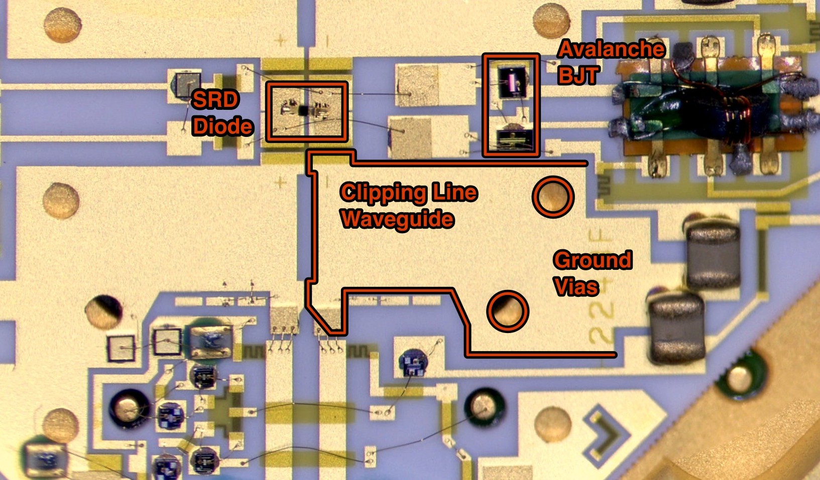 Annotated Photo of the Pulse Generator Section of the SD-24
When a diode conducts current in the forward direction, charge accumulates in its PN junction—a phenomenon known as charge storage. When the diode is suddenly reverse-biased, it takes a finite amount of time to remove this stored charge before the junction can completely shut off. This delay is usually an annoying effect, as it greatly limits the rail-to-rail switching speed of BJTs. For example, the classic 7400-series TTL logic circuits were an order of magnitude more complex and power-hungry than their CMOS counterparts, partly because engineers had to include additional circuitry to mitigate storage effects. Similarly, many BJT operational amplifiers perform poorly when used as comparators for the same reason.
However, researchers at Hewlett-Packard discovered that by using a special doping profile, the diode’s shut-off time could be made extremely short [HP ISSCC]. This discovery led to the development of a new class of discrete components: the Step Recovery Diode (SRD).
Starting with the S-2 sampling head introduced in 1967, Tektronix engineers used an SRD driven by an avalanche-mode BJT to generate the sampling gate pulse. Although detailed time-domain waveforms are hard to find (a measurement worth doing another day), specifications from TekWiki indicate that the device was capable of producing a 150 ps falling edge at up to 30 V[Tekwiki SRD].
The concept is elegant: a carefully designed microstrip transmission line with one end shorted reflects an incoming pulse in such a way that the incident and reflected edges (i.e. we treat the SRD's output as a step function for now) destructively interfere to form a narrow, high-speed pulse, while the slower edges are filtered out. By tuning the geometry of the microstrip, the engineers could control the shape of the pulse to some extent.
This technique first appeared a long time ago in the form of a coaxial cable with one shorted end (which can be found in many vintage testing devices). As the speed requirement increased, the size of this stub have to be reduced accordingly. Eventually, it was implemented as a microstrip line on a high-frequency substrate.
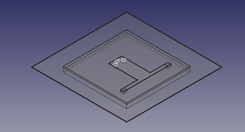
CAD Model of a Clipping Line Pulse Shaper
At a glance, it looks like the line is shorted in the middle, so if we do a DC analysis, the steady state is the entire trace is pulled to ground. However if we look at the transient before the steady state is established, interesting things happen.
Following is an E-field simulation of a clipping line beam shaper created using KiCAD + OpenFEM. The simulation files can be found here
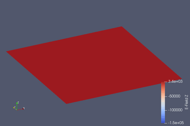
E-field simulation of a clipping line pulse shaper
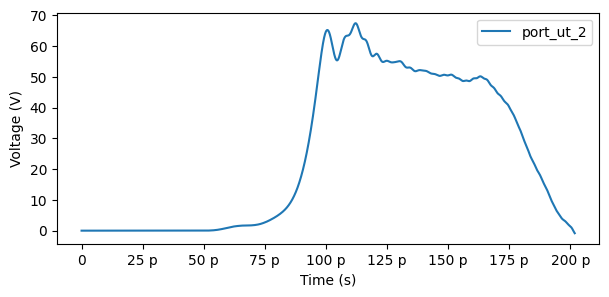
Plot of Port 2 Voltage (Output) when a Step Function is Applied to Port 1 (Input)
As we can see, the reflected wave creates the falling edge of what is supposed to be a step function. The width of the pulse is determined by the length of the clipping line.
In this article, I provided a brief overview of the fundamental building blocks of a high-speed sampling front end. In the next few posts, I will present a detailed reverse engineering of a Tektronix SD-24 sampling head with component-level details. And my end goal is to build a functional equivalent of this sampling head using modern CoTS components. So stay tuned!