
The ultimate goal of this project is to create a complete transceiver system, which means that the system should contain at least an LNA, a mixing element, and an oscillator. (Wait, a "transceiver" should be able to transmit. Maybe I can at lease modulate that oscillator for FM transmitting, but that's not very impressive... I will try to make a proper mixing transmitter if time permits.)
My system is operating at 5GHz. So I'm going to design a 5GHz VCO. But I also want to explore the technology itself a bit more. So I will also make a 24GHz oscillator, a 24GHz "stacked PA", and an on-chip antenna to radiate that out. Let's hope I have enough time to work on that before DDL...
At 5GHz, oscillator design become quite trivial. Somebody demonstrated a 60GHz oscillator on the official Slack channel. But I personally take that with a grain of salt due to how inaccurate the models are at the point and time. For instance they didn't pay much attention to the gate resistance. Which means the reported fmax can be unrealistically high.
fmax is the "maximum power gain". It's a useful metric of RF transistors, essentially giving the designer a rough idea about how fast the transistor can operate to deliver power gain. This number is higher than fT.
$$f_{MAX}=\frac{1}{4\pi}\sqrt{\frac{gm}{r_g\cdot C_{gd}\cdot(C_{gs}+C_{gd})}}=\frac{1}{4\pi}\sqrt{\frac{\omega_T}{r_g\cdot C_{gd}}}$$
But it doesn't mean the oscillator can't produce anything higher than fmax: You can still get some harmonics beyond fmax via multiple mechanisms. It's just that it comes at a loss.
Here comes the dire issue: does the SKY130 technology models gate resistance accurately? I believe it doesn't, as we have seen fmax as high as 200GHz from some simulation results. This is not likely to be true for such a digital-centric 180nm equivalent technology.
What does it take to create an oscillator? Modern control theory can make it quite complicated. But for us RF designers, it usually boils down to some kind of sign-flipped feedback mechanism, which manifests as a phase-shifting network plus a negative resistance.
The architecture I'll be using: cross coupled pair, is a classical negative resistance oscillator. From a differential perspective, the cross-coupled pair looks like:
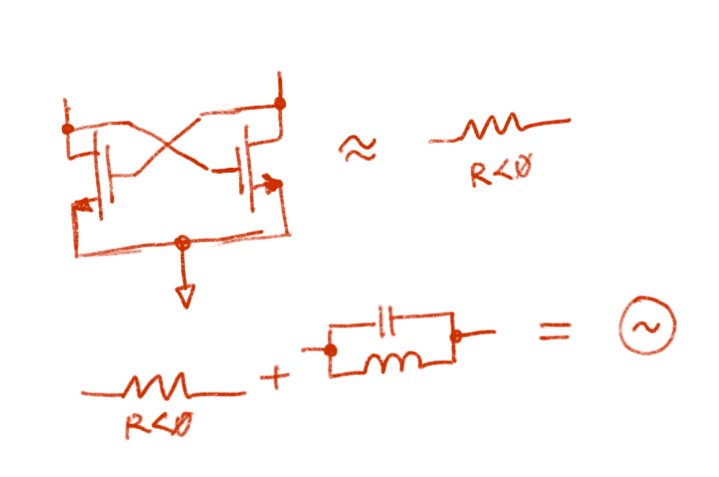
$$Z_{in}\approx-\frac{1}{Gm}=-\frac{2}{gm}$$
At a given frequency point, if the negative resistance is higher than the load, the circuit will begin to oscillate until saturated.
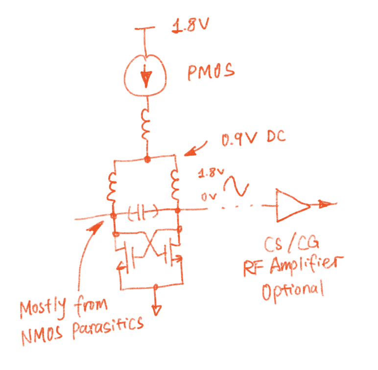
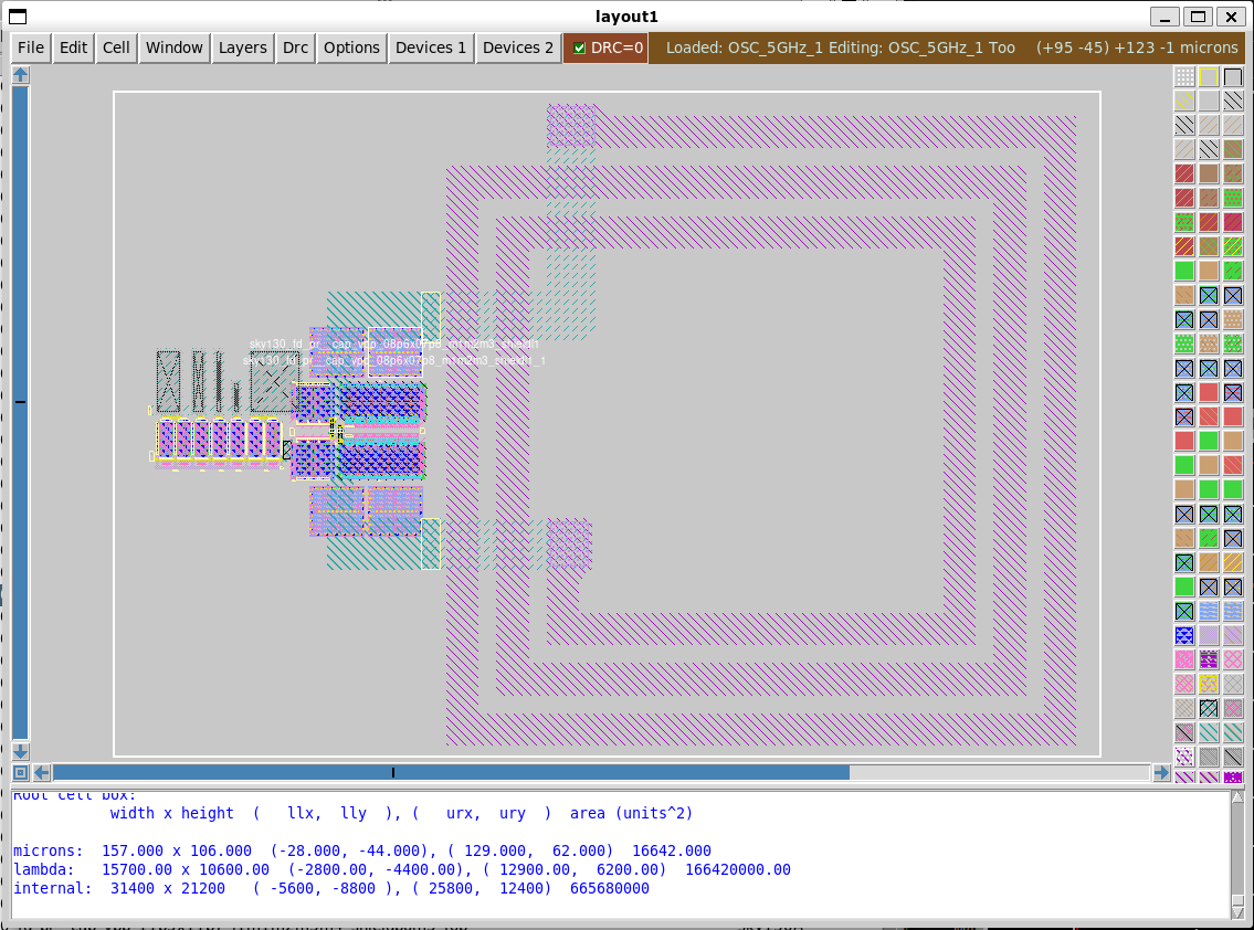
Here's the circuit that does just that: a negative resistance plus a resonant network. This circuit is designed to be operated at 24GHz, with similar captune capability as seen in the previous blog post about the LNA Implementation. Note that there're a lot of weird components (series resistors, caps to the ground, etc) in this diagram. This is my trying to model the parasitics before committing to the layout phase: just to ensure that the circuit should operate under all scenarios.
At 24GHz, PMOS is not fast enough to perform well. So I designed the RF section using exclusively NMOS. PMOS is slow, but it's quieter in terms of noise. I decided to make the current source using PMOS to reduce flicker noise. Because near-DC noise produced by the current source will be modulated on the output RF signal, causing phase noise.
The gate resistance is calculated based on layout "squares" of the poly silicon gate times the square resistance value reported by SKY130.
Based on previous technology-characterization simulations, this transistor should provide a equivalent negative resistance of $$\approx100\Omega$$. This matches pretty well with the simulation. (Oscillation can be sustained when the load is larger than $$150\Omega$$ under all corners).
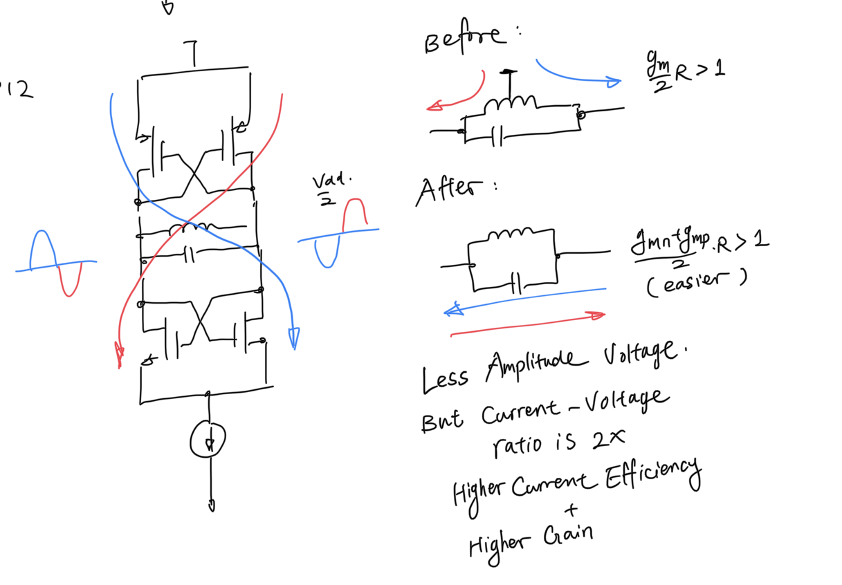
At 5GHz, the PMOS can be used. I went for an fully differential architecture because the PMOS cross coupled pair also contributes to gm, doubling the output capability.
Implementation TBD...
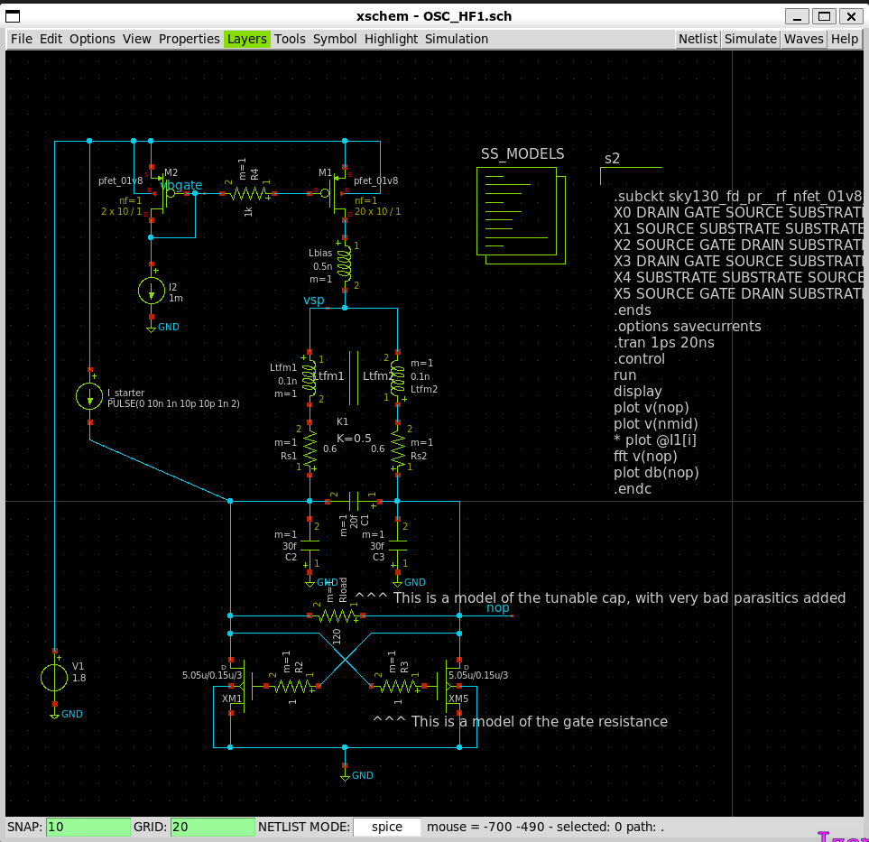
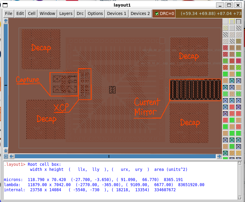
As before, the inductor is designed using ASITIC with a custom-made stack up ASCII file.
To improve the quality factor of the inductor, I added a patterned ground shield (PGS) to this inductor. The goal is to prevent E-field from penetrating into the partially-conductive substrate (which creates loss), and also prevent the B-field from generating vortex current on a sheet of metal.
But the PGS comes at a cost: it messes with your routing, and generally speaking the PGS acts as an capacitor to ground, which doesn't hurt Q, but lowers the self-resonance frequency of the inductor. At very high frequency this structure will start to behave like a capacitor instead of an inductor. But luckily the inductor is sufficient small such that the self-resonant frequency is very high, leaving us quite some room to implement the PGS.
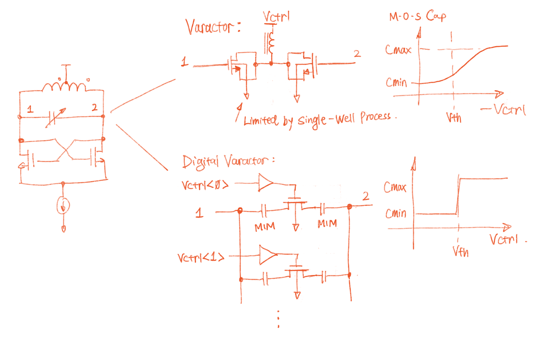
Tunable cap comes in two fashions: analog or digital. Traditionally people use voltage controlled capacitors as the control element as it's able to provide a near-linear control curve. And varactors can be designed in such a way that the parasitic capacitances going to the ground is quite small (as compared to the digital one).
However, if we don't make attempt to limit the output swing, the output of our oscillator will become a large-signal, which means the output voltage itself also modulates the voltage controlled capacitor. This can be disastrous in terms of spectrum purity. If we can afford the extra transistor parasitic, the digital variant eliminates the non-linearity issue, because now the caps are either completely connected or removed, leaving little room for the terminal voltages to affect the capacitance.
Here I'm reusing the tunable cap from the LNA. The parasitics are sufficiently small to not cause any issue.
[]. Behzad Razavi, RF Microelectronics, Chapter 8 - Oscillators
[]. Thomas. H. Lee, The Design of CMOS Radio-Frequency Integrated Circuits,