
This is the first blog post I wrote about our MPW7 project. I will make a dedicated foreword chapter when the chip definition is settled. For now, I'll go over the project briefly.
MPW7 is an abbreviation of the latest silicon shuttle launched by eFabless. Sponsored by Google, eFabless provides free-of-charge silicon service with one limitation: The chip design should be done with and only with the open-source toolchain. I personally believe that the recent open-source movement in the chip design toolchain realm resembles a very promising future for low-to-mid end chip design as a whole (I will probably write another blog post about this in the future). At this point and time the open-source flow is full-featured, but rather difficult to use.
Here's my personal choice of free tools:
Compared to the commercialized tools, the open-source alternatives only offer the minimal function set to complete the flow. The design efficiency and easiness are hardly comparable to that of the commercial ones, forcing the user to rely less on the iterative approach. Even worse, the technology is not well proven:
At this point, the first MPW shuttle turns out to be a disaster due to a bug in clock tree synthesis. Because the chip is only operable when the fixed processor core (that eFabless forces you to use) is able to start up (a terrible design in my opinion), this mistake rendering the entire batch unusable. The second batch is yet to be delivered and tested by the end-users. This is a bad news for us designers because there is absolutely no guarantee in the modeling & simulation accuracy.
This is particularly bad for us RF designers: we rely heavily on the accuracy of transistor capacitance modeling. It's still an open issue that the ngSpice produces highly inaccurate BSIM4 Cgd results under certain scenarios. This is disastrous for RF design. To ensure success, I cheated a bit by verifying the ngspice results against a Cadence one, and employed many on-chip calibration features.

What are we going to design this time? There is something interesting about monolithic integration:
Very low frequency RF (~10MHz) is hard because large inductor & capacitance is hard; Generally speaking the best way to do low-frequency RF is to digitize it and process it in the digital domain.
Very high frequency RF (>10GHz) is hard because parasitic capacitances are everywhere. It demands accurate modeling of capacitances and resistances, and manufacturing precision. SKY130 is not able to provide either of the two.
With those factors taken into consideration. I decided to target 5GHz band, which is commonly required by modern WiFi standards.
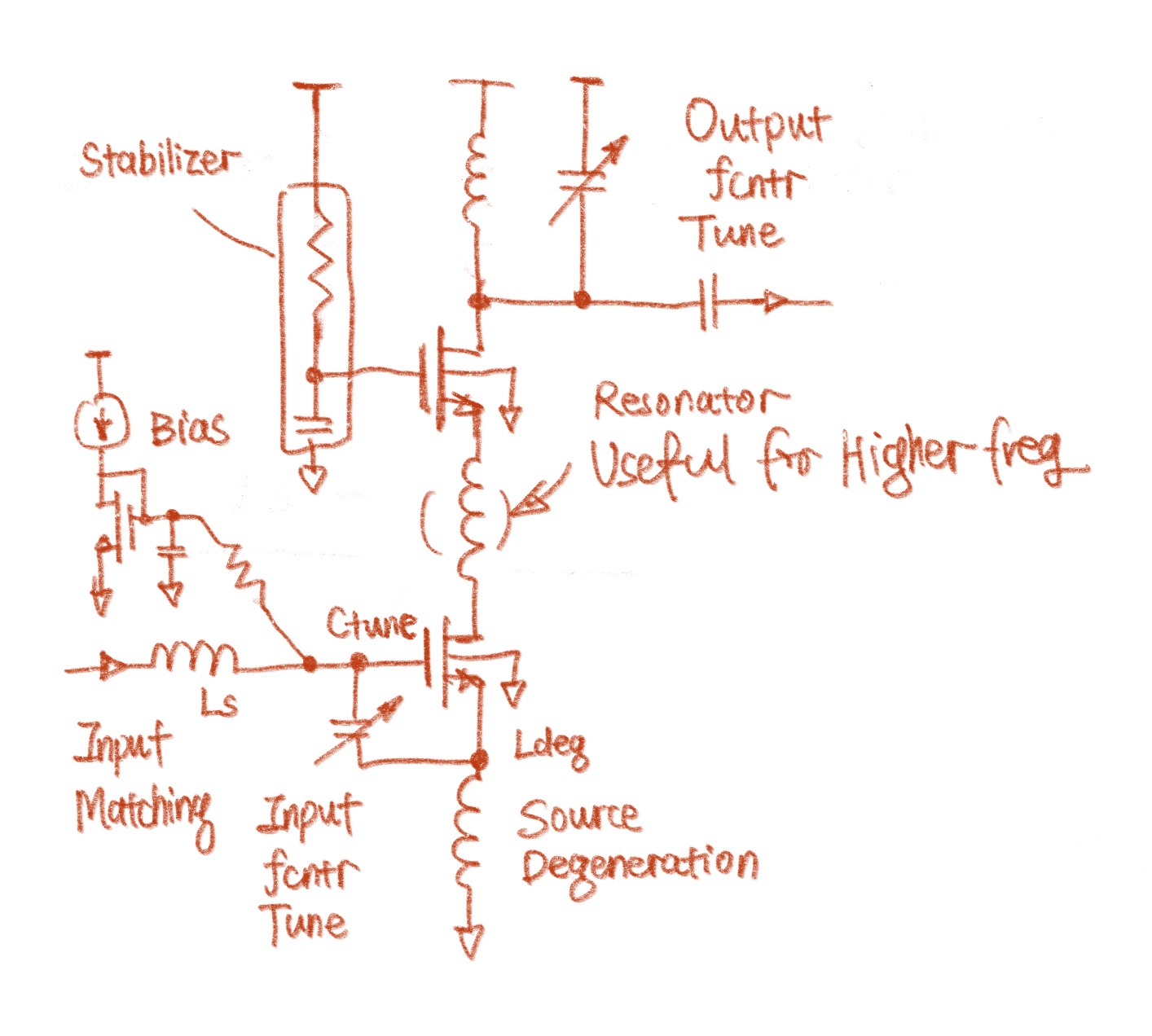
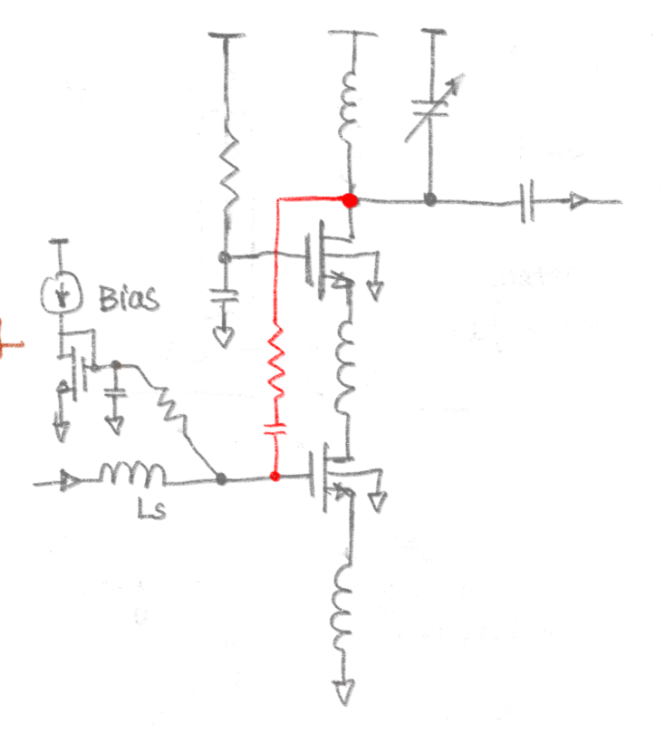
I'm using the most popular cascode architecture for my LNA. There're a couple of key design choices unique to RF as compared to your typical analog design:
The input impedance is:
$$Z_{IN}=j\cdot\omega\cdot L_{s}}+\frac{1}{j\cdot\omega\cdot(C_{gs}+C_{tune})}+\frac{gm\cdot L_{deg}}{C_{gs}+C_{tune}}$$
Where $$C_{tune}$$ is tunable via digital control. $${L_s}$$ is also tunable on the PCB.
Due to manufacturing & modeling inaccuracies, the resonance point of all the L-C pairs may deviate quite a bit on the physical chip. To tame this, two 4-bit digitally tunable caps are inserted, allowing me to tune the resonance point. Instead of relying on the package to provide the inductance (which is common on commercial designs), I decided to do all the inductances on chip because eFabless doesn't provide package modeling at all.
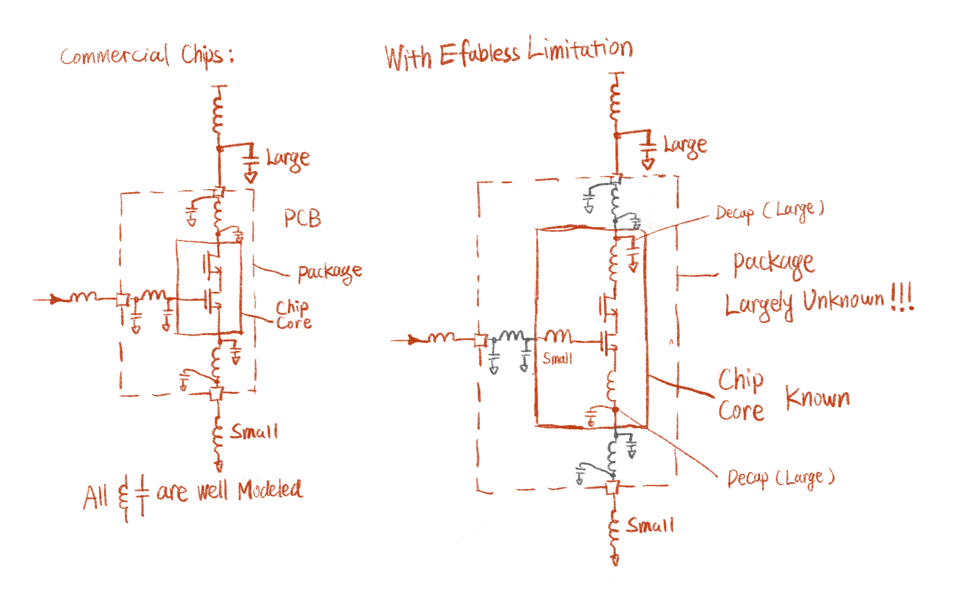
But so far, I haven't touched on the issue of ground bounce. Due to the parasitic inductance and resistance, the internal ground of the chip is not the same as the one outside. This can be a big issue because at RF, the signal trace itself is only doing half of the job while the ground is doing the other half. I have the following solutions for this issue:
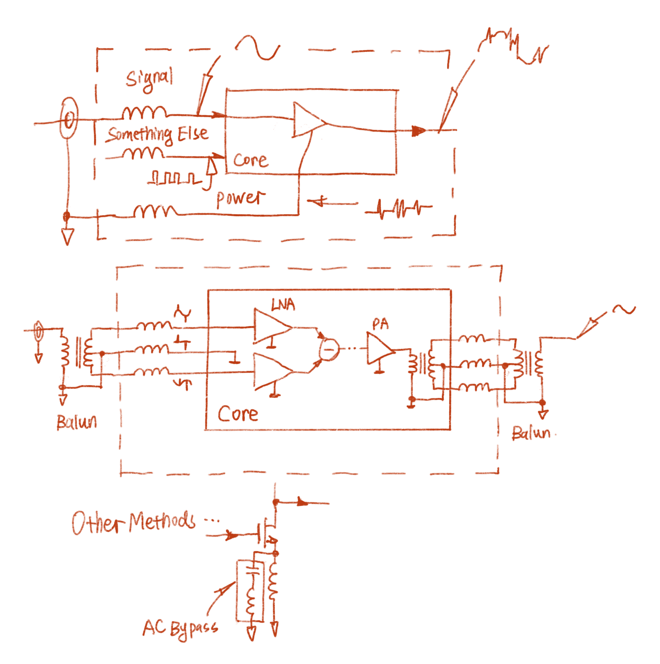
I really don't want to devote more noise budget to an input balun. And differential signaling is easier by comparison: the only thing I need to do is to make my mixer differential, and double the input LNA.
The output tuner is widely used in commercial products, but the input tuner is rare. The reason is:
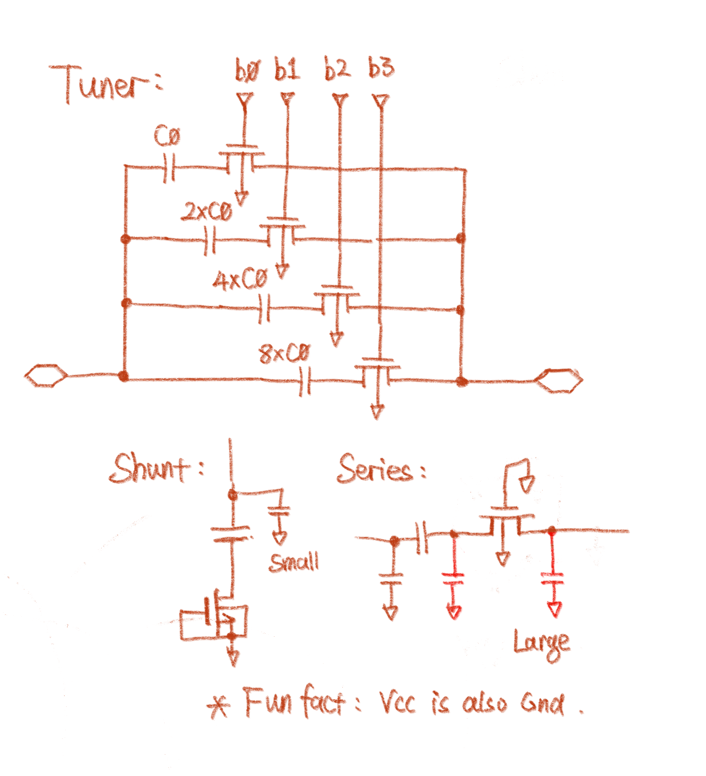
When used as a shunt, most of the parasitics does not load the circuit, doing nothing to our circuit. But when used in series, the parasitics will load our circuit directly. I have considered other tuning mechanism (such as tuning the inductance). But I don't think those designs are any better than this. So let's stick to it.
There're a couple of ways to achieve higher bandwidth. On that, I honestly didn't bother to spend too much time doing calculation. An intuitive way to see it is: when sweept across frequency, you want to stay near the center point of the smith chart for as long as possible.
Here's what a broadband band-pass filter looks like on the smith chart (3rd order Chebyshev):
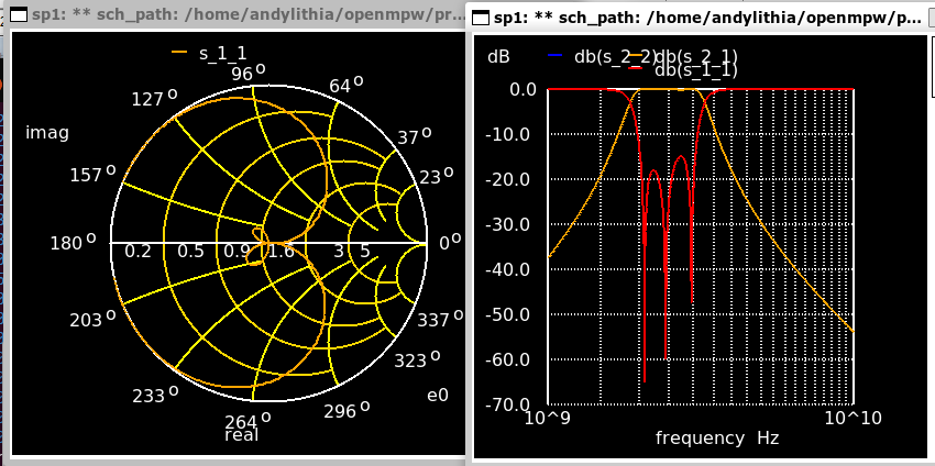
Here're a couple of candidates for increasing the bandwidth of our LNA, some of those solutions come with penalities (which usually boils down to higher power consumption)
By either having a capacitor or a coupled inductor at the input, the LNA S11 can behave like a 2-order Chebyshev. As have been demonstrated by many papers.
First Rev Simulation Summary:
However, it turns out that this architecture is nearly impossible to stabilize at 1~4GHz band. To deal with this problem, a feedback is taken from the output to reduce gain and improve stability
I chained this LNA to obtain extra gain. The input tunable capacitor is removed because the tuning, if necessary, can be done on the PCB.
The transistor lengths are doubled
Both stages are now triple inductor-coupled. This not only improve isolation, but also improve bandwidth.
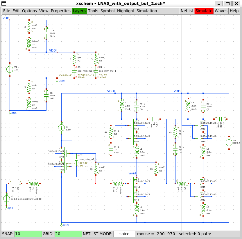
The new version is perfectly stabilized across the entire band of interest
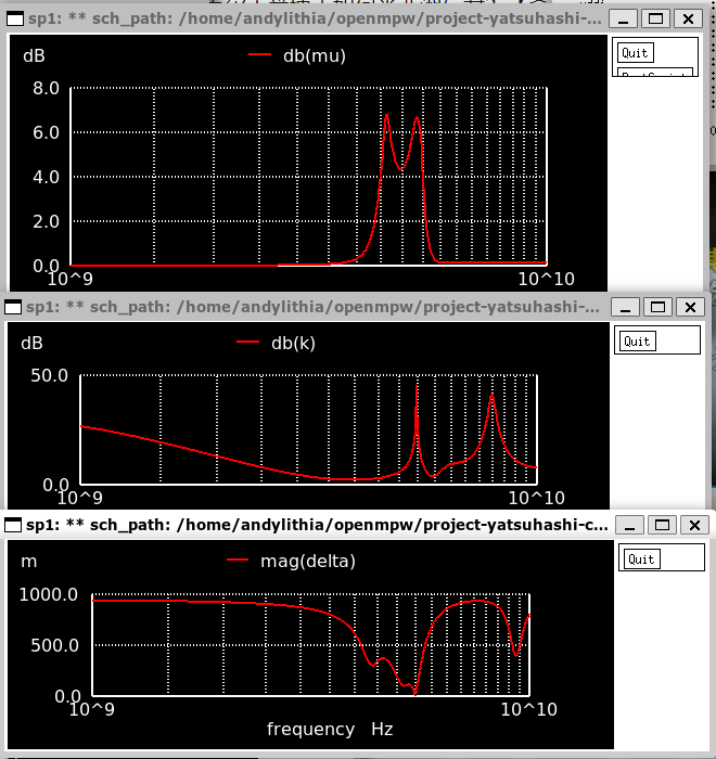
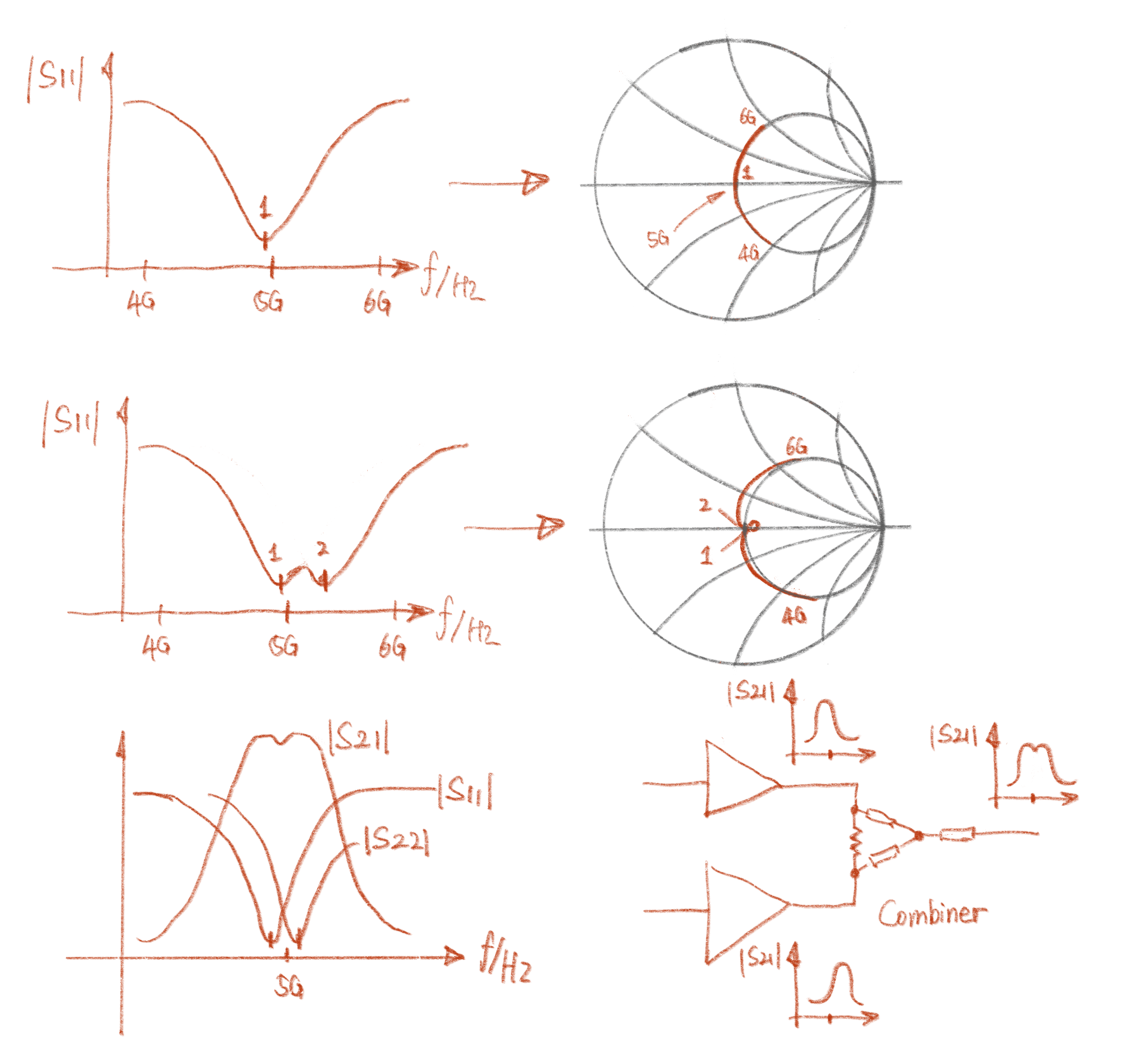
And finally, the wide band SP:
Second Rev Simulation Summary:
I can save a lot of space by using 45-degree chamfered inductors. But Magic VLSI doesn't seem to support it.
Since I'm still very far away from the inductors' self-resonance point. I can implement a patterned ground shielding (PGS) to improve the quality factor of the inductors: As you may know, resistance of a dielectric is directly related to loss. If the E-field is able to penetrate into the silicon semi-conductor substrate, some energy will be lost. By adding some metal stripes (which are highly conductive), the field can be blocked.
I don't want to let RF signal travel too far on my chip. But if I have to, I should use controlled-impedance lines. With that being said, It really is not a big deal for 5GHz. Maybe one day I'll try to do 18GHz, in which case it's absolutely necessary to use CPWs.
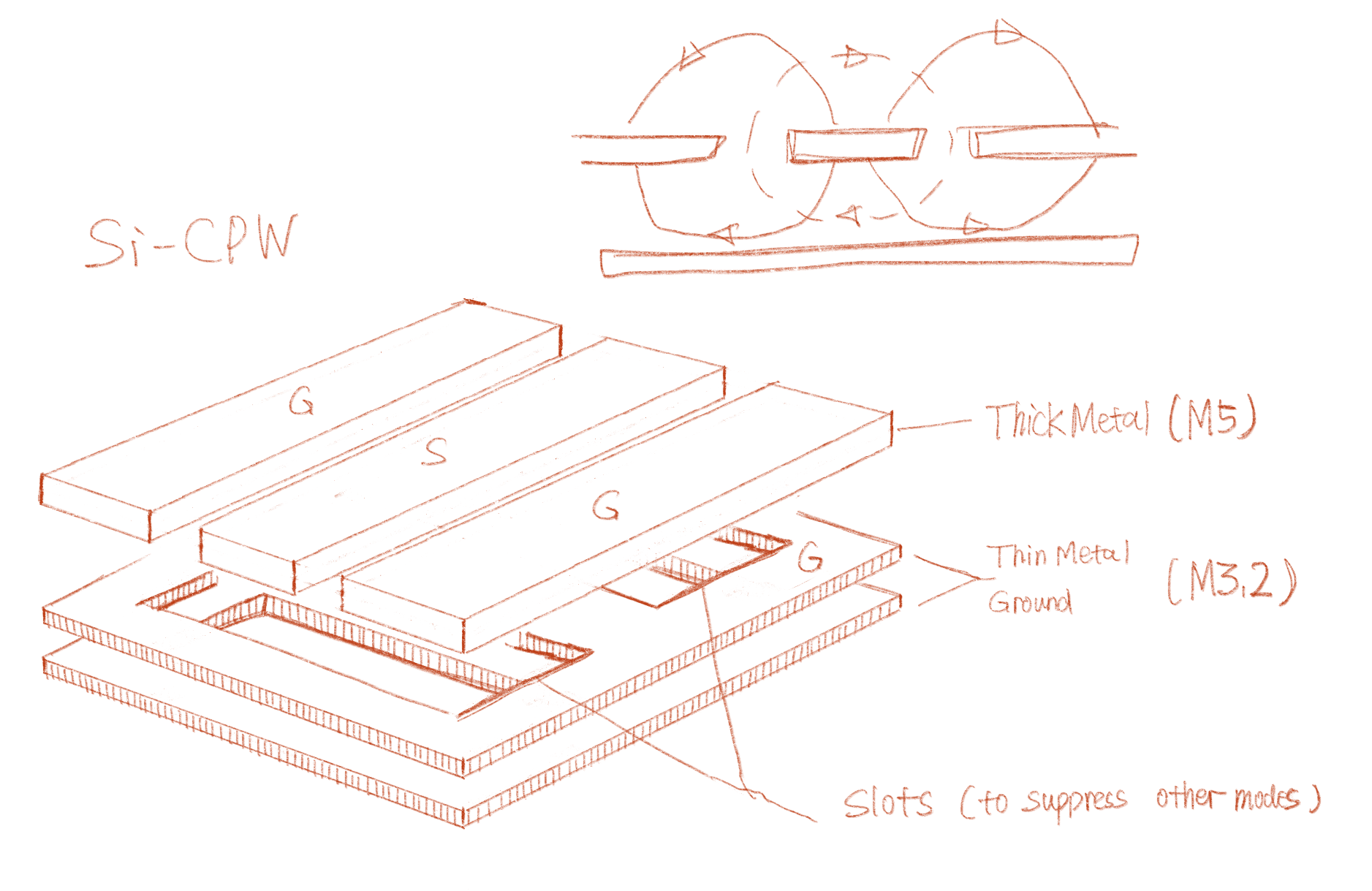
This particular CPW has a characteristic impedance of $$50\Omega$$, but when designing on-chip, I can choose different impedances to miniaturize this structure.