As is discussed in the previous blog post, operational amplifier (OPAMP) is perhaps the most important component of the linear world. An OPAMP comes in many flavors depending on the application: linear, switched, narrow band, wide band, small signal, large signal...
Surprisingly, although we call our project a "mixed-signal" one, we ended up not using any OPAMP at all. The OPAMP I built and simulated should be in the final layout, had we not dropped the pipeline ADC and Σ-Δ ADC. Nevertheless, it's beneficial to take a look at what an OPAMP is made of in a modern process.
The application I proposed demands fully differential operation and high bandwidth.
Performance Target:
The current mode OPAMP is quite popular in low-voltage CMOS processes. It offers a wide output swing, compact size (no miller compensation), and most importantly, no internal high-impedances. The third point makes this type of OPAMP (ideally) a single-pole system, thus fairly easy to stabilize.
In practice, due to all kinds of capacitive coupling, when the gain is set too high the OPAMP can still get into oscillation. But luckily for us the gain is easily tunable by modifying the current mirror ratio.
$$A_V\approx\frac{gm_{M1}\cdot K\cdot r_{out}}{1+s\cdot r_{out}\cdot C_{load}}$$
Where K is the width ratio of M4 vs. M3.
$$ \begin{circuitikz} \ctikzset{logic ports=ieee, logic ports/scale=0.7,} \ctikzset{tripoles/pmos style/emptycircle} \ctikzset{tripoles/mos style/arrows} \draw (0,0) node[nmos](M1p){M1p}; \draw (M1p.S) to [short, -*] ($(M1p.S)+(1,0)$); \draw (M1p.S) to [short, -] ($(M1p.S)+(2,0)$); \draw ($(M1p.S)+(2,0)$) node[nmos, anchor=S, xscale=-1](M1n){\scalebox{-1}[1]{M1n}}; \draw ($(M1p.S)+(1,0)$) node[nmos, anchor=D](M2){M2}; \draw (M1p.G) to [short, -o] ++(-0.25,0) node[left]{$Vi_p$}; \draw (M1n.G) to [short, -o] ++(+0.25,0) node[right]{$Vi_n$}; \draw (M2.G) to [short, -o] ++(-1,0) node[left]{$V_{bias}$}; \draw (M2.S) to [short, -*] ($(M2.S)+(0,-1)$); \draw ($(M2.S)+(-5,-1)$) to [short, -] ($(M2.S)+(5,-1)$); \draw (M1p.D) to [short] ++(0,0.5) node[pmos, anchor=D](M3p){M3p}; \draw (M1n.D) to [short] ++(0,0.5) node[pmos, anchor=D, xscale=-1](M3n){\scalebox{-1}[1]{M3n}}; \draw (M3p.G) --++(-0.25,0) to [short, *-] ++(0,-1) to [short, -*] ++(1.25,0); \draw (M3n.G) --++(+0.25,0) to [short, *-] ++(0,-1) to [short, -*] ++(-1.25,0); \draw (M3p.G) --++(-0.5, 0) node[pmos, anchor=G, xscale=-1](M4p){\scalebox{-1}[1]{M4p}}; \draw (M3n.G) --++(+0.5, 0) node[pmos, anchor=G](M4n){M4n}; \draw (M4p.D) --++(0,-3) node[nmos, anchor=D, xscale=-1](M5p){\scalebox{-1}[1]{M5p}}; \draw (M4n.D) --++(0,-3) node[nmos, anchor=D](M5n){M5n}; \draw (M5n.S) node[circ]{} ++(0,0); \draw (M5p.S) node[circ]{} ++(0,0); \draw (M5n.G) -- (M5p.G); \draw ($(M5p.G)+(1,0)$) to [short, *-] ++(0,-1.5) to [short, -o] ++(-3,0) node[left]{$V_{CMFB}$}; \draw ($(M4p.S)+(-1.5,0)$) to [short, -] (M4p.S) to [short, *-] (M3p.S) to [short, *-] (M3n.S) to [short, *-*] (M4n.S) --++(1.5,0); \draw ($(M4p.D)+(0,-1.5)$) to [short, *-o] ++(-1,0) node[left]{$V_{outn}$}; \draw ($(M4n.D)+(0,-1.5)$) to [short, *-o] ++(+1,0) node[right]{$V_{outp}$}; \end{circuitikz} $$
The most dire issue of a fully differential amplifier is that, information is encoded in the difference between the two differential lines, but nothing decides the common-mode biasing point for both of them. This in practice means that with PVT variations, the DC biasing of the output node can be all over the place. We need to devise a feedback mechanism that stabilizes the common-mode voltage to a healthy level (in the sense that all the transistors are correctly biased). This kind of feedback is known as "Common-Mode Feedback", or CMFB for short.

$$ \begin{circuitikz} \ctikzset{logic ports=ieee, logic ports/scale=0.7,} \ctikzset{tripoles/pmos style/emptycircle} \ctikzset{tripoles/mos style/arrows} \draw node[pmos](M6b){M6b}; \draw (M6b.G) --++(0,-1) to [short, *-o] ++(-3,0) node[](n1){} to [short, *-] ++(0,1) node[pmos, anchor=G](M6a){M6a}; \draw (n1) to [short, -o] ++ (-1,0) node[left]{$V_{bias,p}$}; \draw (M6b.G) --++(0,-1) --++(3,0) node[](n2){} --++(0,1) node[pmos, anchor=G](M6c){M6c}; \draw (M6b.S) to [short, *-*] (M6c.S) --++ (1,0); \draw ($(M6a.S)+(-3,0)$) to [short, -*] (M6a.S) -- (M6b.S); \draw (M6a.D) --++(0,-0.5) node[nmos, anchor=D](M7a){M7a}; \draw (M7a.G) to [short, -o] ++(-0.25,0) node[left]{$V_{I1}$}; \draw (M6c.D) --++(0,-0.5) node[nmos, anchor=D, xscale=-1](M7d){\scalebox{-1}[1]{M7d}}; \draw (M7d.G) to [short, -o] ++(0.25,0) node[right]{$V_{I2}$}; \draw (M6b.D) to [short, -*] ++(0,-0.5) node[](n3){}; \draw (n3) --++(-1,0) node[nmos, anchor=D,xscale=-1](M7b){\scalebox{-1}[1]{M7b}}; \draw (n3) --++(+1,0) node[nmos, anchor=D](M7c){M7c}; \draw (M7b.G) to [short, *-] ++(0,-1) to [short, -o]++(-5,0) node[left](){$V_{REF}$}; %\draw (M7b.G) to [short, -o] ++(0,0) node[left]{$V_{REF}$}; %\draw (M6b.D) --++(0,-1) node[nmos, anchor=D](M7b){M7b}; %\draw (M7b.G) to [short, -o] ++(0,0) node[left]{$V_{REF}$}; %\draw (M6b.D) to [short, -*] ++(0,-0.75) to [short,-o]++(4,0) node[right]{$V_{CMFB}$}; \draw (M7a.S) to [short, -*] ++(1,0) node[](n4){} --(M7b.S); \draw (n4) node[nmos, anchor=D](M8a){}; \draw ($(M8a.G)+(-0.25,0)$) node[anchor=south](){M8a}; \draw (M7c.S) to [short, -*] ++(1,0) node[](n5){} --(M7d.S); \draw (n5) node[nmos, anchor=D](M8b){M8b}; %\draw (n5) node[nmos, anchor=D](M8b){M8b}; \draw (M8b.G) -- (M8a.G) to [short, -o] ++(-2,0) node[left](){$V_{bias,n}$}; %\draw (n5) -- (M7c.S); \draw ($(M8a.S)+(-5,0)$) to [short, -*] (M8a.S) to [short, -*] (M8b.S) --++(3,0); \end{circuitikz} $$
At such an advanced (65nm) technology node, it's generally easier to implement higher frequency circuits (in terms of $$f_T$$) with smaller power consumption. But it also brings a worse $$gm\cdot r_{out}$$ compared to the older technologies. This is a bad news if given the same UGB, we want to achieve a high DC gain (commonly required by ADCs, etc) instead of a high bandwidth.
Increasing the current mirror ratio is not an option because it increases $$C_L$$ and hurts matching. Cascode is possible, but decreases voltage head room. One popular solution is to add internal positive feedback as shown below:
$$ \begin{circuitikz} \ctikzset{logic ports=ieee, logic ports/scale=0.7,} \ctikzset{tripoles/pmos style/emptycircle} \ctikzset{tripoles/mos style/arrows} \draw (0,0) node[nmos](M1p){M1p}; \draw (M1p.S) to [short, -*] ($(M1p.S)+(3,0)$); \draw (M1p.S) to [short, -] ($(M1p.S)+(6,0)$); \draw ($(M1p.S)+(6,0)$) node[nmos, anchor=S, xscale=-1](M1n){\scalebox{-1}[1]{M1n}}; \draw ($(M1p.S)+(3,0)$) node[nmos, anchor=D](M2){M2}; \draw (M1p.G) to [short, -o] ++(-0.25,0) node[left]{$Vi_p$}; \draw (M1n.G) to [short, -o] ++(+0.25,0) node[right]{$Vi_n$}; \draw (M2.G) to [short, -o] ++(-1,0) node[left]{$V_{bias}$}; \draw (M2.S) to [short, -*] ($(M2.S)+(0,-1)$); \draw ($(M2.S)+(-7,-1)$) to [short, -] ($(M2.S)+(7,-1)$); \draw (M1p.D) to [short] ++(0,0.5) node[pmos, anchor=D](M3p){M3p}; \draw (M1n.D) to [short] ++(0,0.5) node[pmos, anchor=D, xscale=-1](M3n){\scalebox{-1}[1]{M3n}}; \draw (M3p.G) --++(-0.25,0) to [short, *-] ++(0,-1) to [short, -*] ++(1.25,0); \draw (M3n.G) --++(+0.25,0) to [short, *-] ++(0,-1) to [short, -*] ++(-1.25,0); % Positive feedback node \draw ($(M3p.S)+(1.75,0)$) node[pmos, anchor=S, xscale=-1](Mcp){\scalebox{-1}[1]{Mcp}}; \draw ($(M3n.S)-(1.75,0)$) node[pmos, anchor=S](Mcn){Mcn}; \draw (Mcp.D) to [short, -*] ++(0,-0.25); \draw (Mcn.D) to [short, -*] ++(0,-0.25); \draw ($(M3p.D)+(0,-0.25)$) --++ (2.5,0) to [short] (Mcn.G); \draw ($(M3n.D)+(0,-0.25)$) --++ (-2.5,0) to [short] (Mcp.G); \draw (M3p.G) --++(-0.5, 0) node[pmos, anchor=G, xscale=-1](M4p){\scalebox{-1}[1]{M4p}}; \draw (M3n.G) --++(+0.5, 0) node[pmos, anchor=G](M4n){M4n}; \draw (M4p.D) --++(0,-3) node[nmos, anchor=D, xscale=-1](M5p){\scalebox{-1}[1]{M5p}}; \draw (M4n.D) --++(0,-3) node[nmos, anchor=D](M5n){M5n}; \draw (M5n.S) node[circ]{} ++(0,0); \draw (M5p.S) node[circ]{} ++(0,0); \draw (M5n.G) -- (M5p.G); \draw ($(M5p.G)+(1,0)$) to [short, *-] ++(0,-1.5) to [short, -o] ++(-3,0) node[left]{$V_{CMFB}$}; \draw ($(M4p.S)+(-1.5,0)$) to [short, -] (M4p.S) to [short, *-] (M3p.S) to [short, *-] (M3n.S) to [short, *-*] (M4n.S) --++(1.5,0); \draw ($(M4p.D)+(0,-1.5)$) to [short, *-o] ++(-1,0) node[left]{$V_{outn}$}; \draw ($(M4n.D)+(0,-1.5)$) to [short, *-o] ++(+1,0) node[right]{$V_{outp}$}; \end{circuitikz} $$
This OPAMP is able to deliver 50dB gain, 500MHz UGB at ~200uW total power consumption as seen in schematic simulation. But rather unfortunately, our final circuit doesn't contain any OPAMP at all.
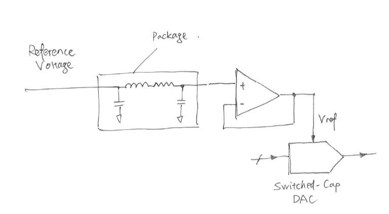
I do think that adding an internal voltage buffer at the internal voltage reference nodes are useful, but if the OPAMP for some reason doesn't work, our chip will be unable to receive (a fairly high current consumption) reference DC voltage. To bet on the safe side, we decided not to implement the OPAMP buffer.