
Chip design is entirely about signal manipulation. To carryout an action, one has to come up with a intricate structure made with elements from two worlds: the linear world known as Analog, and the switched world known as digital.
The topic of this blog post: Comparator, is the most simple and important building block that bridges the two worlds. In particular, if we somehow have access to a sampling clock, a positive-feedback comparator known as StrongARM is the most popular option.
To get the question out of the way: What is so different about comparators as opposed to an OPAMP?
From the input perspective, they are the same: All that we want is an amplifier that amplifies the difference between two input terminals, as fast and quiet as the current budget allows.
But an OPAMP is intended to work in an negative feedback loop, so the output stage design has to prioritize linearity, stability, etc. For comparators, we want the output stage to be as fast as possible. A comparator doesn't need to have a very linear transfer characteristic, but it does need to provide minimal hysteresis (which means high linearity in another way).
In our application, the comparator is expected to operate on a sampled signal. Naturally StrongARM becomes a nobrainer.
$$ \begin{circuitikz} \ctikzset{logic ports=ieee, logic ports/scale=0.7,} \ctikzset{tripoles/pmos style/emptycircle} \ctikzset{tripoles/mos style/arrows} \draw (0,0) node[nmos](M1){}; \draw (M1.G) node[anchor=south] {M1}; \draw (M1.S) node[circ]{} to ($(M1.S)+(5.5,0)$); \draw ($(M1.S)-(5.5,0)$) to [short, -] (M1.S); \draw (M1.D) --++(0,0.5) coordinate(M1D); \draw (M1D) to [short, *-] ($(M1D)-(1.5,0)$) node[nmos, anchor=S](M2p){M2p}; \draw (M1D) -- ($(M1D)+(1.5,0)$) node[nmos, anchor=S, xscale=-1](M2n){\scalebox{-1}[1]{M2n}}; \draw (M2p.D) --++(0,1) coordinate(M2PD); \draw (M2n.D) --++(0,1) coordinate(M2ND); \draw (M2PD) node[nmos, anchor=S, xscale=-1](M3p){\scalebox{-1}[1]{M3p}}; \draw (M2ND) node[nmos, anchor=S](M3n){M3n}; \draw (M3p.D) to [short, *-] ($(M3p.D)+(0.5,0)$) -- (M3n.G); \draw (M3n.D) to [short, *-] ($(M3n.D)-(0.5,0)$) -- (M3p.G); \draw (M3n.D) --++(0,1.5) node[pmos,anchor=D](M4n){M4n}; \draw (M3p.D) --++(0,1.5) node[pmos,anchor=D, xscale=-1](M4p){\scalebox{-1}[1]{M4p}}; \draw (M4p.D) to [short, *-] ($(M4p.D)+(0.5,0)$) -- (M4n.G); \draw (M4n.D) to [short, *-] ($(M4n.D)-(0.5,0)$) -- (M4p.G); \draw (M3p.D) --++ (0,1) node[circ]{} --++ (-2,0) coordinate(von) --++ (0,0.5) node[pmos, anchor=D](M5p){M5p}; \draw (M3n.D) --++ (0,1) node[circ]{} --++ (2,0) coordinate(vop) --++ (0,0.5) node[pmos, anchor=D, xscale=-1](M5n){\scalebox{-1}[1]{M5n}}; \draw (vop) to [short, *-o] ++(2,0) node[right]{$Vo_+$}; \draw ($(M3p.D)+(0,0.5)$) to [short, *-] ++(5,0) to [short, -o] ++(2,0) node[right]{$Vo_-$}; \draw (M5n.G) |- (M1.G); \draw (M1.G) -| (M5p.G) to [short, *-o] ++(-0.5,0) node[left]{$\overline{precharge}$}; \draw (M5n.S) --++ (2,0); \draw (M5n.S) to [short, *-] (M4n.S) to [short, *-] (M4p.S) to [short, *-] (M5p.S) to [short, *-] ++(-2,0); \draw (M2p.D) to [short, *-] ++(0.75,0) node[nmos, anchor=D, rotate=90, xscale=-1](M6){\scalebox{-1}[1]{M6}}; \draw (M6.S) to [short, -*] (M2n.D); \draw (M6.G) to [short, -] ++(-2,0) node[not port, anchor=out](G1){}; \draw (G1.in) to [short, -*] ++(-1.25,0); \draw (M2p.G) to [short, -o] ++(-2.5,0) node[left]{$Vi_+$}; \draw (M2n.G) --++ (0,-1.25) to [short, -o] ++(-7.5,0) node[left]{$Vi_-$}; \end{circuitikz} $$
Fig 1. StrongARM Schematic
The latch is such a robust design, that we don't need to put in too much serious effort to make it work properly. But with that being said, we still made a number of iterations to make sure that the comparator will not limit the performance of our ADC.
We sweeped parameters to ensure the following performance criteria is satisfied.
Because we don't care too much about speed (we're talking about 65nm, any thing can run at 1GHz easily, let alone the StrongARM), we focused mostly on the monte-carlo simulation.
The result of such a simulation looks like this:
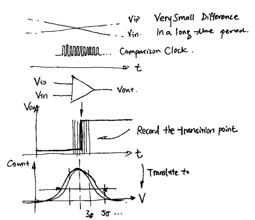 Monte Carlo Simulation Setup
Yes, I can't show the actual result, but we choose 5σ as an acceptable range. We want the 5σ range (whose unit is V) to be smaller than the LSB of our ADC.
Next let's talk about layout, I want to make it very compact, and cross-place the p/n transistor pairs as much as possible.
The schematic, when laid down, becomes this:
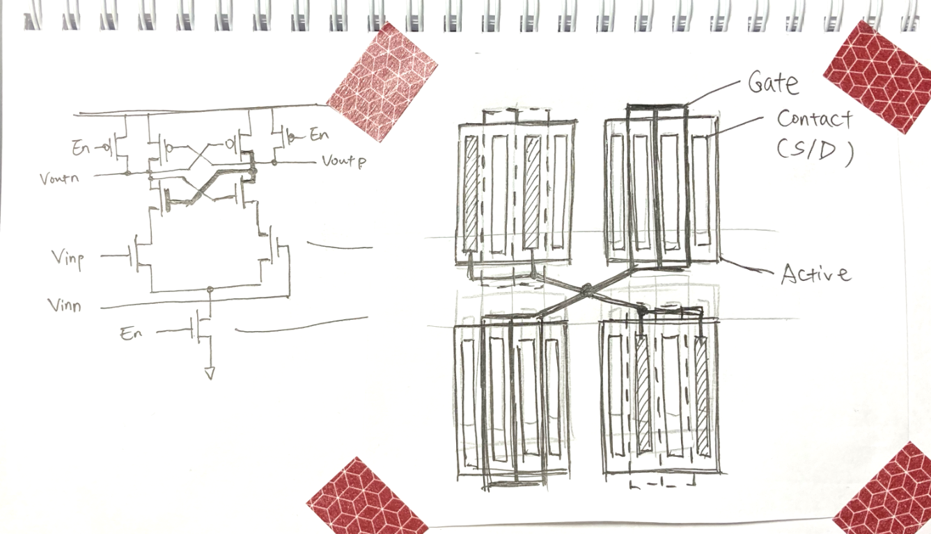 The layout of two transistors
One net is high lighted
Note that, despite on the right hand side I have four instances drawn, it's actually only two transistors (M3p, M3n). Each half is further broken into 2 parts to enable X-shaped placement, which improves matching against both X & Y gradients.
As you can imagine, the routing is quite tedious. A more extreme way to place it is known as "interdigital", where the two halves are very tightly placed, usually with in the same active region.
Actually, when doing the monte-carlo simulation, the simulator assumes that the transistors are entirely independent. Which is not the case when laid down: the transistors in close proximity has similar characteristic. So I believe the fabricated chip can perform much better than the 5σ number reported.